In today’s electronics-driven world, printed circuit boards (PCBs) form the foundation of nearly every device we use — from smartphones and laptops to industrial control systems and IoT devices. Behind every sleek gadget lies a sophisticated process of PCB assembly and circuit board manufacturing that ensures performance, reliability, and scalability.
This article explores the key steps in modern PCB fabrication and assembly, the technologies that make it possible, and how engineers can optimize design-to-production workflows for faster, more efficient output.
Understanding the Core of PCB Assembly
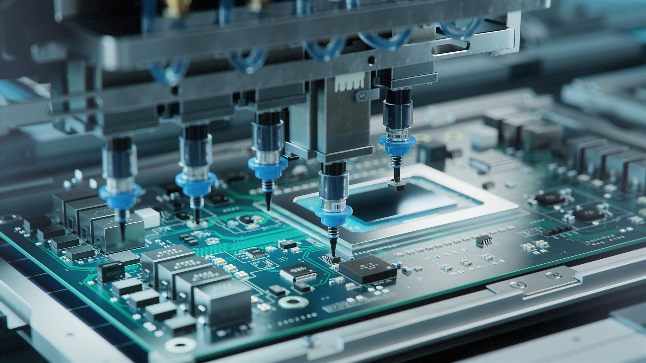
At its simplest, PCB assembly refers to the process of populating a bare circuit board with all the electronic components required for the device to function. The process typically involves soldering resistors, capacitors, integrated circuits, and connectors onto copper traces according to the circuit design.
High-quality PCB assembly is more than just attaching components — it’s about precision, consistency, and long-term reliability. Manufacturers use a combination of automated machinery and quality control systems to ensure every solder joint is perfect and that each component is placed with sub-millimeter accuracy.
For a deeper insight into how professional assembly lines manage flexible and rigid board production, visit pcb assembly for detailed information on flex PCB and hybrid solutions used in today’s most advanced electronics.
The Importance of Design for Manufacturability (DFM)
Before any physical assembly begins, engineers must ensure the PCB design meets manufacturing constraints — a concept known as Design for Manufacturability (DFM). Poor DFM can result in short circuits, signal loss, or even total board failure during production.
Some of the most critical DFM considerations include:
-
Trace Width and Spacing: Ensuring proper signal integrity and avoiding electrical interference.
-
Via Placement: Strategic via positioning prevents mechanical stress and improves current flow.
-
Component Orientation: Consistent component alignment simplifies automated assembly and inspection.
-
Thermal Management: Efficient heat dissipation avoids hotspots and prolongs component life.
By integrating DFM early in the design phase, manufacturers can significantly reduce production costs and improve yield rates.
The Step-by-Step Circuit Board Manufacturing Process
While PCB assembly deals with component placement, the circuit board manufacturing process focuses on creating the base structure that supports those components. It’s a highly controlled sequence of mechanical, chemical, and thermal steps that transform raw materials into a functioning board.
Here’s a simplified overview of the process:
-
Design & Gerber File Preparation
Engineers generate Gerber files that define copper layers, drills, and solder mask data — the blueprint for fabrication. -
Material Selection & Lamination
Layers of copper and substrate (FR4, polyimide, or flexible materials) are laminated together under heat and pressure. -
Imaging & Etching
A photoresist is applied and exposed to UV light, defining the copper traces. Unwanted copper is etched away, leaving conductive pathways. -
Drilling & Plating
Precision drilling creates vias and mounting holes. These are then plated with copper to ensure electrical connectivity between layers. -
Solder Mask & Silkscreen
The green solder mask protects copper traces from oxidation and shorts, while the silkscreen adds component labels and logos. -
Electrical Testing & Inspection
Automated Optical Inspection (AOI) and flying probe tests verify continuity, impedance, and correct trace geometry. -
Surface Finish Application
Depending on the application, finishes like HASL, ENIG, or OSP are added to improve solderability and shelf life.
To explore these steps in greater detail, including illustrations and advanced tips, check out this circuit board manufacturing step-by-step guide that breaks down each stage of PCB fabrication with visual examples.
Surface Mount vs. Through-Hole Assembly
There are two primary techniques used in PCB assembly:
-
Surface Mount Technology (SMT):
Components are placed directly onto the surface of the PCB using solder paste and reflow ovens. SMT enables miniaturization and higher circuit density — essential for smartphones, wearables, and high-speed computing. -
Through-Hole Technology (THT):
Components have leads that pass through drilled holes and are soldered on the opposite side. Though bulkier, THT remains valuable for high-power or high-stress applications like automotive systems or industrial controllers.
Many modern boards use a hybrid approach, combining SMT for efficiency and THT for mechanical stability.
The Rise of Flexible and Rigid-Flex PCBs
Traditional rigid boards are giving way to flexible and rigid-flex PCBs, especially in compact or dynamic applications. Flexible PCBs use bendable substrates like polyimide, allowing them to fit in tight or curved enclosures. These are common in foldable phones, medical wearables, and aerospace instrumentation.
Rigid-flex designs combine both rigid and flexible layers — offering durability with space efficiency. As product designs become more compact, such hybrid configurations are revolutionizing how engineers think about hardware architecture and interconnect design.
Quality Control and Testing Standards
Every PCB must pass through multiple inspection stages before reaching the customer. Manufacturers perform tests like:
-
Automated Optical Inspection (AOI) for visual defects
-
X-ray Inspection for hidden solder joints (especially BGAs)
-
In-Circuit Testing (ICT) to validate electrical performance
-
Functional Testing (FCT) to simulate real-world operating conditions
These rigorous procedures ensure every board meets IPC-A-610 and ISO 9001 quality standards, ensuring reliability in mission-critical applications.
Trends Shaping the Future of PCB Manufacturing
The PCB industry continues to evolve rapidly, driven by miniaturization, environmental regulations, and automation. Some emerging trends include:
-
Additive Manufacturing (3D-Printed PCBs): Offering rapid prototyping and reduced waste.
-
High-Frequency & High-Speed PCBs: Supporting 5G, radar, and high-speed data systems.
-
Eco-Friendly Fabrication: Water-based etchants, recyclable materials, and halogen-free laminates.
-
AI-Driven Quality Control: Machine learning algorithms predict defects and optimize yield.
Manufacturers adopting these innovations gain a significant competitive edge in both speed and sustainability.
Conclusion
From initial schematic design to the final solder joint, PCB assembly and circuit board manufacturing represent the backbone of modern electronics innovation. With advancements in materials, automation, and precision engineering, today’s boards are smaller, faster, and more reliable than ever.
Whether you’re designing for consumer electronics, industrial systems, or cutting-edge IoT applications, understanding the full lifecycle of PCB production empowers you to build smarter, more efficient, and future-ready devices.
To dive deeper, explore detailed insights into pcb assembly and the circuit board manufacturing process — both essential resources for engineers, designers, and hardware innovators looking to stay ahead in this rapidly evolving industry.